July 11, 2025
Your Process. Our Expertise. – Demo Capabilities for Challenging Substrates
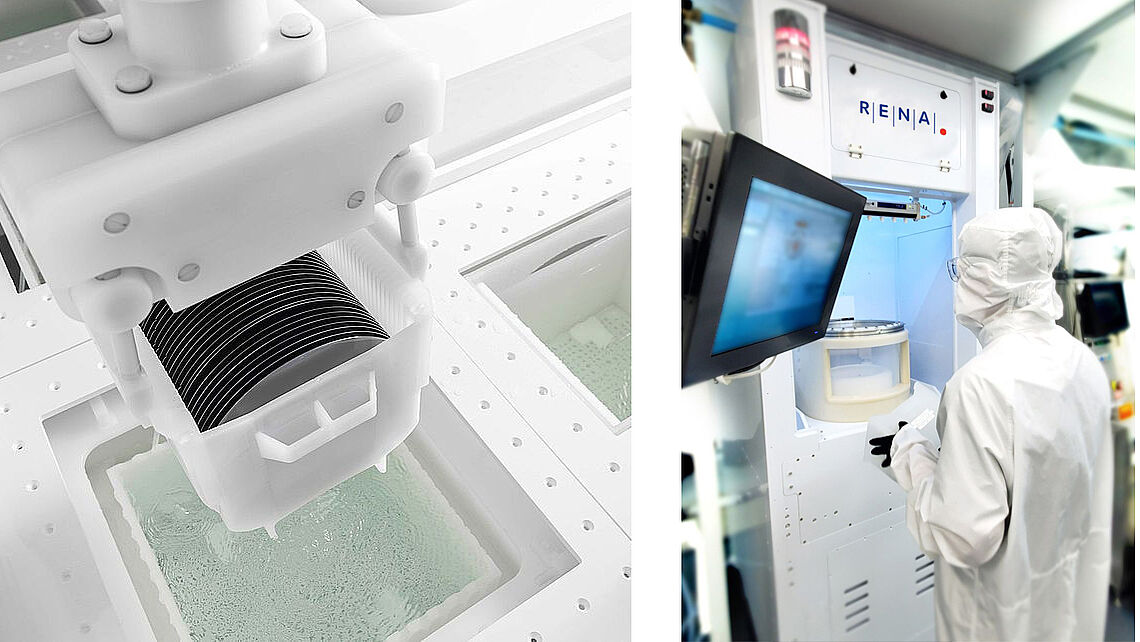
Looking for Semiconductor Demo Capabilities for Silicon, Compound Semiconductors, or Glass Wafers/Panels?
At RENA, we offer robust demo and foundry support for process validation and optimization — tailored to your substrate and application needs.
Whether you're working with silicon, compound semiconductors, or glass wafers/panels, our dedicated demo labs are equipped to help you validate and refine your wet processing steps with precision and flexibility.
Our Core Capabilities Include:
- Standard cleans, etches, and resist strips
- Damage-free batch metal lift-off (MLO) – ideal even for fragile wafers like GaAs and InP
- TGV (Through Glass Via) etching for advanced glass panel applications
- Wet strain relief etching for SiC substrates
- Porous layer formation on Si, SiC, and III-V semiconductors
- Specialized post-CMP cleaning for critical surface quality
Demo Lab Equipment & Process Scope:
- Fully equipped for up to 200 mm wafer processing
- Support for batch immersion, spray, and single wafer applications
- In-house cleanliness, critical dimension (CD), and optical metrology capabilities
Ready to validate or fine-tune your next semiconductor process?
Contact us to explore how our demo services can accelerate your development with confidence.
» Click here to get to our wet chemical solutions
» Are you interested in our wet chemical systems? Please contact our sales team.
