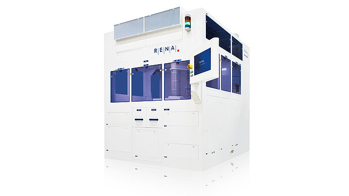
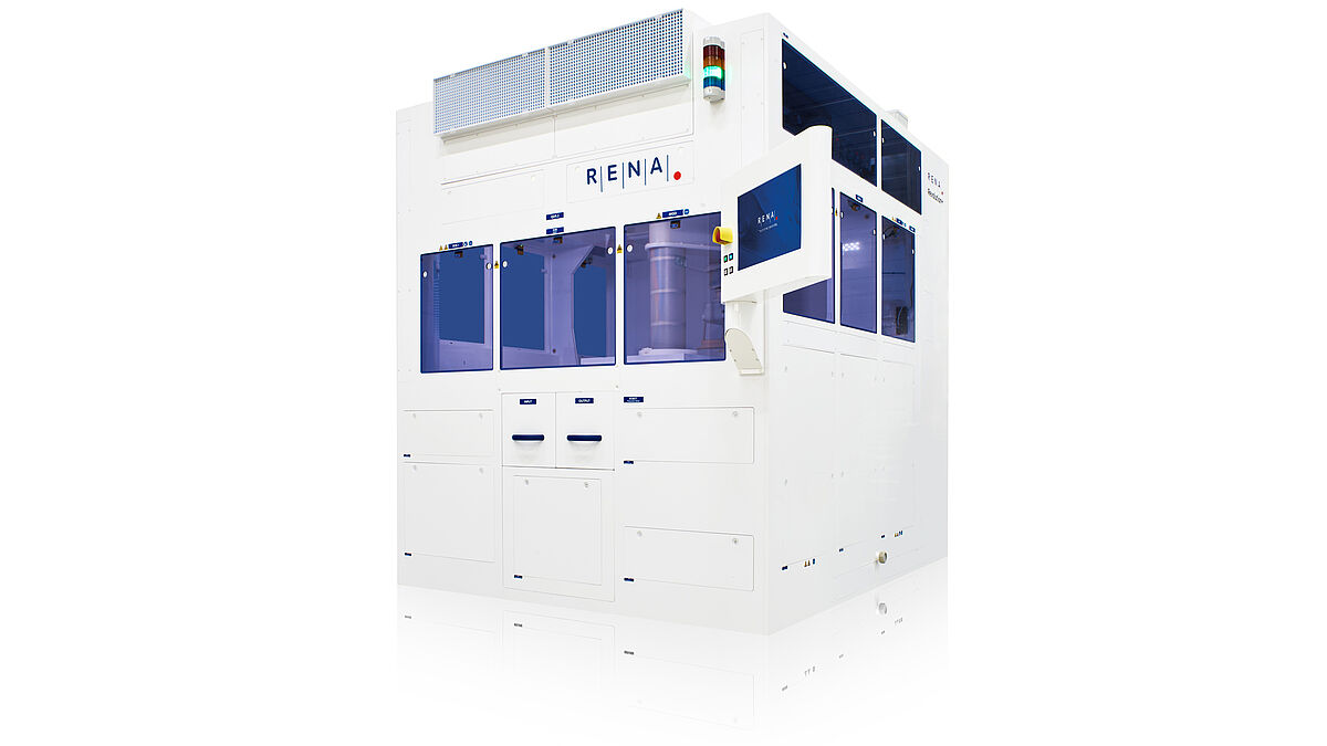
Glass Wafer Processing

Wafers, made of glass, are the basis of the modern micro system technology. Glass has many advantages as a material such as high chemical and heat resistance, high electrical isolation, biocompatibility, large optical transition range as well as low optical absorption. Due to these properties, glass wafers are widely used in conventional microfabrication processes. RENA offers small scale tools for wet processing of glass wafers.

Glass Wafer Cleaning

For any processing technology we need clean glass wafer. Cleaning of glass wafers is a very crucial step for high efficiency in manufacturing of components out of glass or even successful processing. Depending on glass wafer handling conditions, glass wafer can evidence various type of contamination such as organic contamination or inorganic in form of particles. One requires obviously different cleaning procedures to remove these various types of contamination. Depending on further processing steps, glass wafer will also require different wet processing steps. It may be preparation for bonding process or for coating application for example. RENA can serve customers in selection of appropriate cleaning protocol and provide a corresponding tool.

RENA offers:

  • Cleaning with organic solvents
  • Cleaning with aqueous solutions
  • RCA cleaning protocols
  • Surface activation and conditioning

RENA glass processing

Microfabrication process allows the creation of diverse structures in a glass wafer. To achieve good quality in a structuring process, initial cleaning process is of crucial importance. RENA can offer glass etching with different media depending on process requirements and type of glasses. Depending on the customers’ needs, processing tools for glass wafers can also contain baths for glass etching and resist stripping.

Process steps such as chrome etching can be integrated in a process sequence for structuring of a chrome layer. RENA also offers equipment for etching of commonly used metals in a fabrication process, such as gold and nickel. The individual processing steps of glass wafers can be freely adjusted to the required throughput and specific customer needs.

  • Glass etching
  • Metal etching / Chrome etching
  • Resist stripping

Applications

Optics

Thousands of micro-optics components can be fabricated in parallel on a glass wafer using microfabrication process. Optical components such as lenses, mirrors, beam splitters and gratings can mostly be used in photonics, the semiconductor industry, or the medical field. Refractive and diffractive micro-optical elements are used for precise beam shaping. Micro-optics also play an important role in medical devices such as endoscopes, as well as laser-based devices and fiber communication networks.

Microfluidics

Many microfluidic systems are fabricated out of glass with microfabrication process. Microfluidic systems have become essential elements for biomedical instrumentation for diagnostics. Being transparent under a wide wavelength range, glass is the first candidate for micro bioanalytical devices such as microcapillary electrophoresis or devices for cell trapping or sorting. Microfluidic systems with sophisticated channel structure find their applications in devices for point of need testing (PON), and flow cells for single molecule handling of DNA for next generation sequencing (NGS).

Sensors

The technology for the microfabrication of glass is gaining in importance because more and more glass substrates are currently being used to fabricate MEMS devices. Today it is already implemented as a mature solution, such as acceleration and pressure sensors. Patterned wafers with cavities which can be obtained through etching are used to encapsulate the pressure sensor die. The encapsulation is done by using a wafer level packaging (WLP) approach.
 

Read more about MEMS and sensors

Customized Solutions: Wet processing systems

Wet Processing Platform for glass wafer
Wet Processing Platform for glass substrates

Advanced cleaning solutions

  • For highest performance and challenging environments in the Glass, MedTech, Pharma and Semiconductor industries
  • Water- and solvent-based
  • Cleanroom, ATEX, GMP

Looking back at over 20 years of expertise in cleaning applications for various substrates, RENA offers advanced processing solutions for glass wafers like glass etching for diverse industries and challenging environments. With us you will find customized solutions to implement optical components, microfluid processes and sensors, such as a pressure sensor, in the best possible way.

Our glass wafer batch processing and glass etching tools deliver the highest performance for the Glass, MedTech, Pharma, Advanced Optics and Semiconductor sectors. They fulfill cleanroom, ATEX and GMP requirements and are designed for water as well as organic solvent-based processes.

Technical Sales Manager
Felix Fink
ResponsibleResponsible for the following countries:
Worldwide