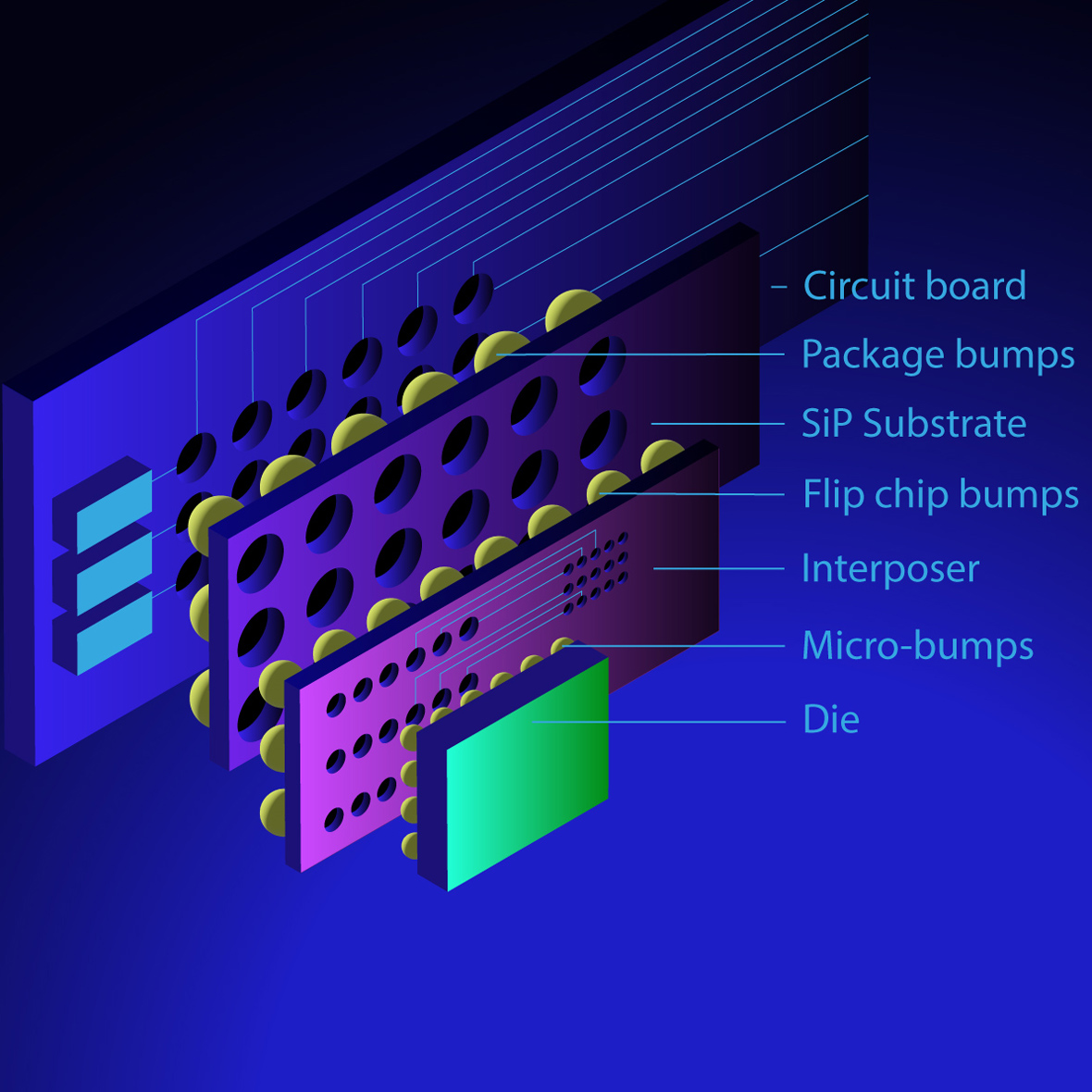
Through glass vias (TGV)
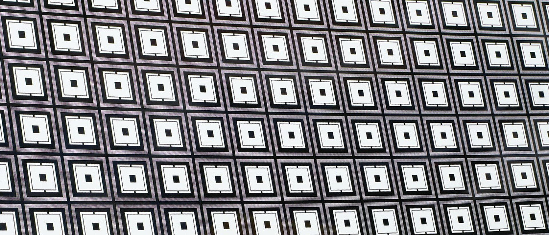
The demand for miniaturization, multifunctional and connected devices including smartphones, wearables, and Internet of Things has been growing very fast. This miniaturization and functionality leads to the increased demand for high density and high bandwidth interconnections. The concept of 2.5-D and 3-D IC integration for packaging is a key component to achieve next-generation performance requirements and to apply to commercial products. The ultrahigh number of I/O connections is becoming available using interposers.

 wafer")
 panel")


 taper angle")