Electroplating - advanced electrochemical deposition for semiconductor manufacturing
One of the key steps in semiconductor manufacturing is the electrochemical deposition of metallic interconnects which form electrical circuits. Plating is a fast and cost effective way for metallic connections in device manufacturing and advanced packaging.
The semiconductor segment of RENA offers high-quality manual and automated electroplating platforms for a wide variety of plating applications, such as Damascene, Barrier diffusion layer, Under bump metallization (UBM), Bumping, Pillars, Through silicon vias (TSVs) and Through glass vias (TGVs). RENA ‘s manual and automated electroplating platforms deliver superior process results in device fabrication and packaging to manufacture MEMS sensors, CMOS image sensors, LEDs, RF and photonic devices.
RENA’s advanced fountain technology guarantees optimal flow dynamics and precise electric field control. These features provide customers with an optimal electrolyte exchange rate at the substrate surface as well as outstanding uniformity and yield even at high plating rates.
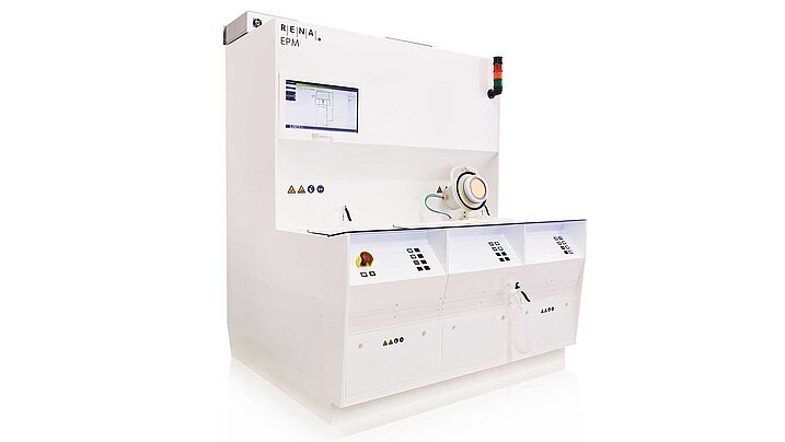
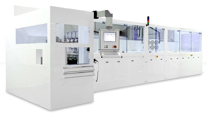
Our manual electroplating station, EPM, has compact footprint and is ideal for R&D applications and small scale production. Next to the Fountain, EPM includes a quick dump rinse (QDR) tank for subsequent surface cleaning On the other hand, RENA’s automated plating platform, EPA, is suitable for large scale production and enables customers to perform multiple plating processes, simultaneously. Surface preparation steps such as resist removal, seed layer etch, cleaning and drying ensure a smooth high productivity process sequence.
The modular designed electroplating platforms are highly flexible. Wafer substrates from 75 mm to 200 mm can be handled and fast substrate size changes are guaranteed. Numerous types of alloys as well as pure metals are reliably plated, like Nickel (Ni), gold (Au), tin (Sn), cupper (Cu), silver (Ag), tin silver (SnAg), indium (In) among other. These metals can be electrochemically deposited on various substrate materials such as Si, silicon carbide (SiC), gallium arsenide (GaAs), gallium nitride (GaN), indium phosphide (InP), glass, sapphire and alumina (Al2O3).