EPM2 - Advanced manual electrochemical deposition

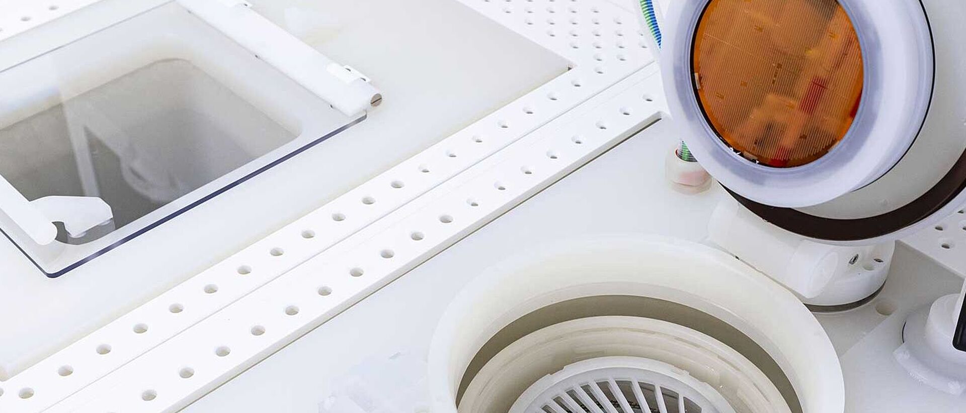
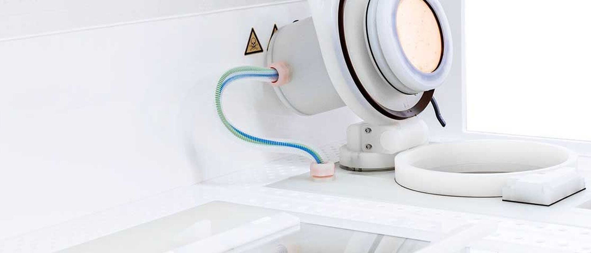
Highest flexibility is required for pure metal and alloy deposition in the Microelectronic, Optoelectronic & Photonic chips market and its wide range of plating applications. The EMP 2 is a compact electro-plating system for semiconductor device manufacturing and packaging applications, such as UBM, Bumping, Cu pillars, TSVs, Blind vias, RDL, Micro Forming and more. Homogeneous deposition at highest plating rates is ensured by optimized electrolyte flow and electrical field control in the fountain system. The plating tool operates manually and can be installed in R&D environments as well as in small scale production.

Overview of RENA EPM 2 system benefits

​​​​​​

Flexibility

  • Different substrate sizes
  • Adjustable wafer thickness
  • Wide range of materials
  • Flexible recipe management
     

High quality plating performance

  • Plating materials:
    Pure metals: Cu, Au, Ni, In, Sn, Pt 
    Alloys: SnAg, PbSn, FeNi
  • Inert or soluble anode
  • DC or forward/reverse 
    pulse plating
  • Edge exclusion: < 3mm
  • 360° Ti contact pin arrays

Process stability & control

  • Control of process parameters like wafer rotation, electrolyte flow, temperature and current
  • pH-control
  • Automated dosage
  • Conductivity measurement for 
    QDR rinse module
     

Operator & service safety

  • Good accessibility
  • Easy maintenance
  • Drag out rinse included in plating process module

EPM 2 | 100 F

  • 1 fountain process chamber

EPM 2 | 101 F

  • For lab applications
  • 1 Fountain process chamber
  • 1 Quick dump rinse

EPM 2 | 201 F

  • For small scale production and labs
  • 2 Fountain process chambers
  • 1 Quick dump rinse in between process chambers

Flexibility for a wide range of applications

The RENA EPM 2 system was designed to be integrated easily into research and institute environments as well as production facilities with a focus on very small-scale production. The low floor space, modular design, and option to add on extra process modules for pre-treating, etching, and drying guarantee the flexibility customers expect when it comes to electroplating.

RENA is a strong partner for electrochemical deposition applications for the device manufacturing for optoelectronic, microelectronic devices and Photonic Chips in the semiconductor business. Wafer sizes from 2 to 8 inch are feasible in our tools, further substrate sizes and geometries are possible. Depending on the application requirements different plating technologies such as vertical rack, fountain, cup and fully customized plating can be applied.

Downloads

no downloads found.
Theo-Moissidis-Head-of-Sales
VP Sales
Theo Moissidis
ResponsibleResponsible for the following countries:
Worldwide