
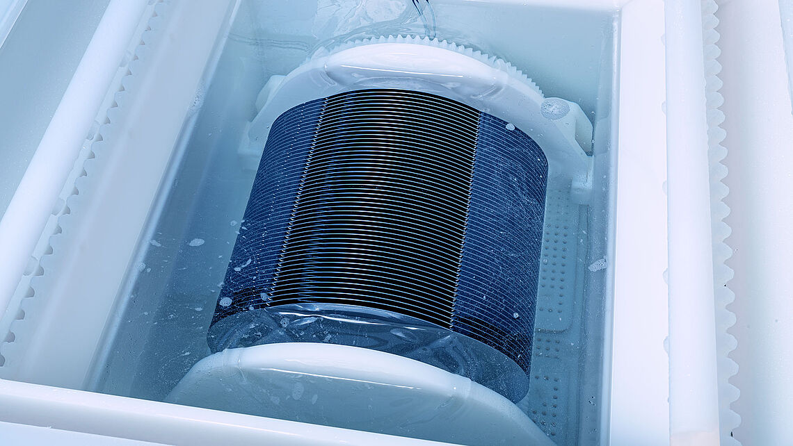
For your applications in Front End of Line (FEoL) or Back End of Line (BEoL) production, whether you are manufacturing sensors, MEMS or RF-components – every semiconductor wafer is running through several wet processing steps. The most common processes are etching, polishing, cleaning and stripping.
Besides other approaches the immersion tools are an established solution for high volume semiconductor production.


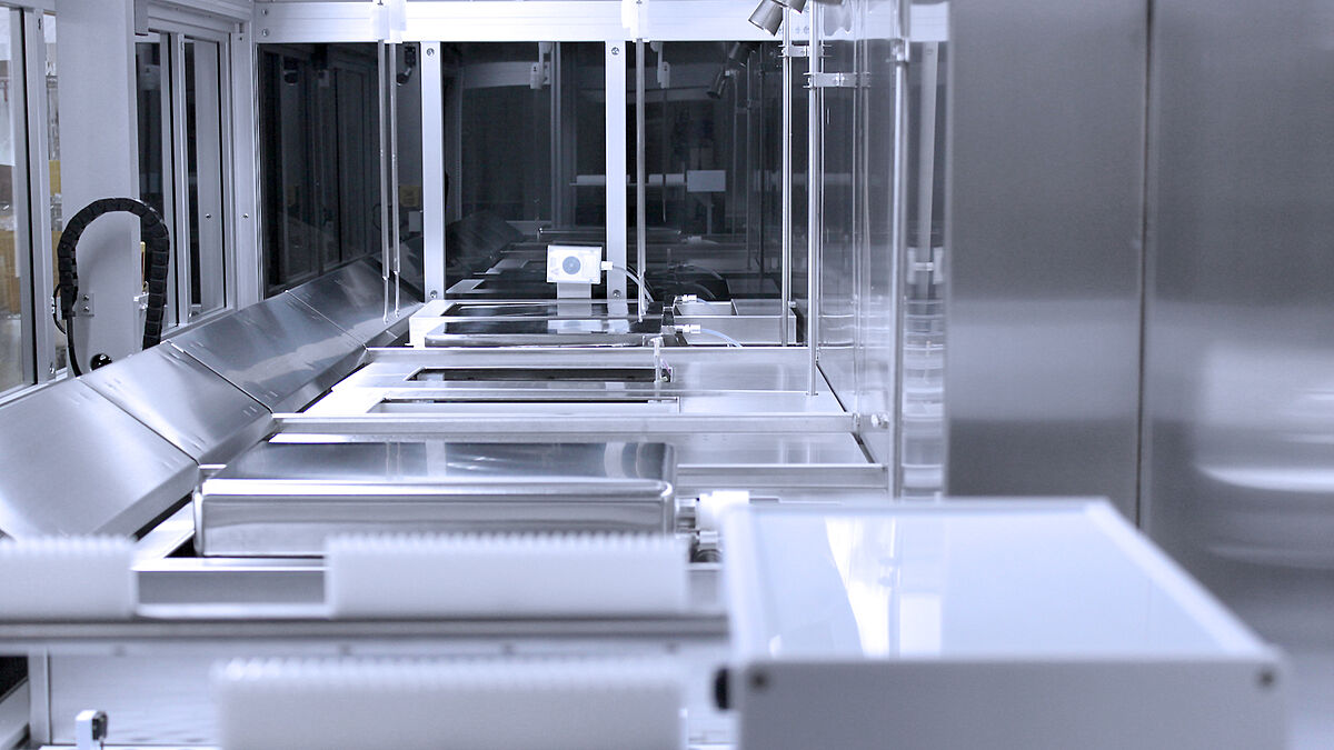
Evolution – Fully Automatic Wet Processing
The "Evolution" wet bench is an industry proven, linear semiconductor processing system dedicated to wet processes like etching, cleaning, and stripping. High yield yet outstanding surface quality is key for this tool. Keeping the cost of ownership in mind it comes with a sophisticated dosing system to reduce chemistry consumption to a minimum. If required, the FlexView scheduler for simultaneous lot processing optimizes throughput.
It`s modular design allows for customized and process sequences and easy configuration. Multi-step processing in specialized process tanks, like ultrasonic and megasonic tanks, cascades or quick dump rinsing tanks can be performed according to the process requirements. Dry-in and dry-out with various drying solutions as well as interfaces like FOUP, FOSB and SMIF are mandatory.
All RENA systems are compliant to the SECS/GEM interface.
Evolution Highlights
- Full-Auto, dry-in and dry-out operation
- 100 mm to 300 mm wafer sizes
- Up to 100 wafers per lot
- Simultaneous lots & recipes
- Chemical spiking, filtration and re-circulation
- Class 1 mini-environment
- Acid & solvent solutions
- Integrated automatic bulk chemical system
- Tailored to customer specification and upgradeable

Suiting your semiconductor application
The substrate material can make the difference. Whether you are manufacturing MEMS, Logics, Sensors, LED, RF, IC, Power Electronics, Automotive or Optical components, we can cover you. With our tools you can handle pure Silicon wafers as well as glass- and compound wafers like Silicon Carbide, Gallium Nitride or Gallium Arsenide. Depending on the substrate material processing of different wafer sizes ranging from 100 – 300 mm wafers can be performed.

Substrate Materials
- Si
- Glass
- Compound Semiconductors
GaN, GaAs, SiC

