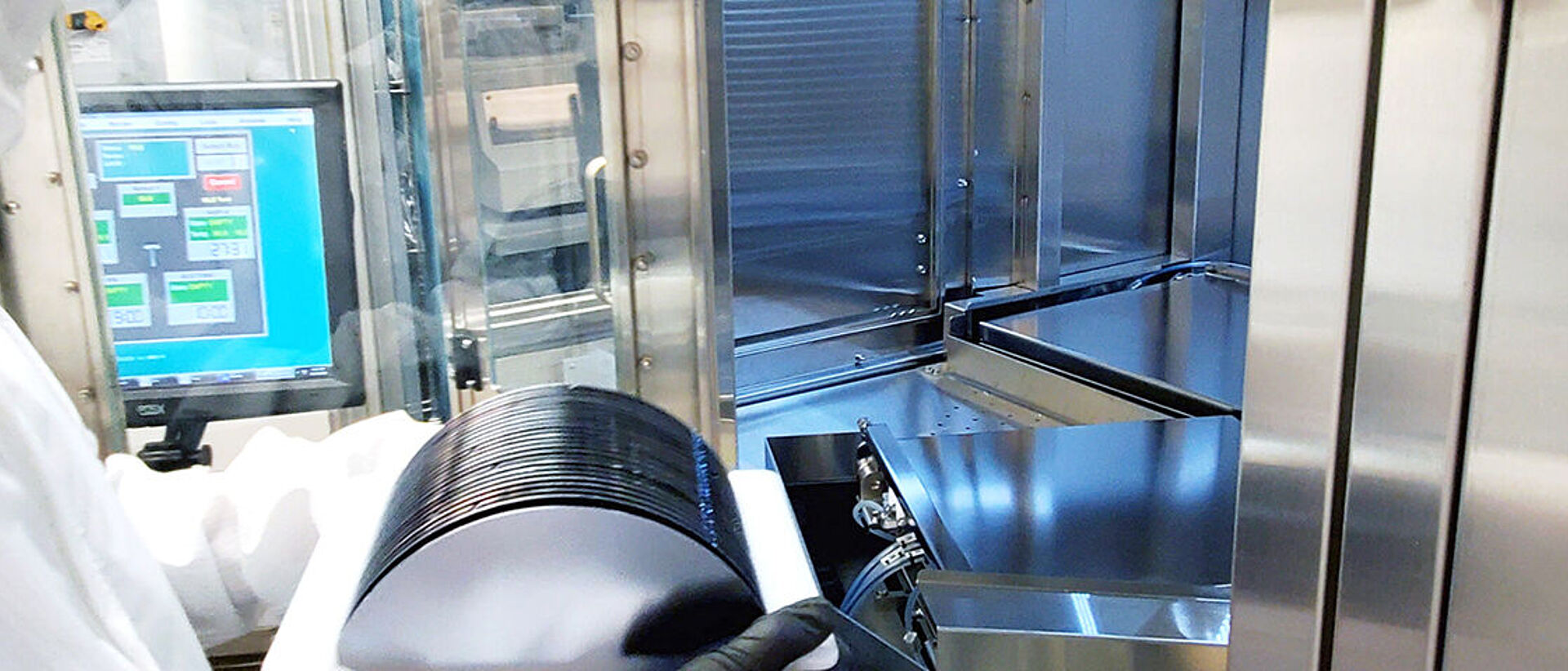
Wet Solutions for your Lab or Production
Designed for R&D - proven in mass production


Whether you're producing MEMS, logic circuits, sensors, LEDs, RF components, ICs, power electronics, automotive parts, or optical components, we have you covered. Our tools are capable of handling pure silicon wafers as well as glass and compound wafers, including silicon carbide, gallium nitride, and gallium arsenide. We can process various wafer sizes ranging from 100 mm to 300 mm, depending on the substrate material.