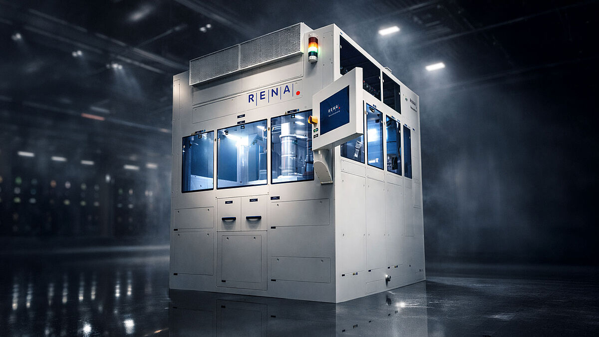
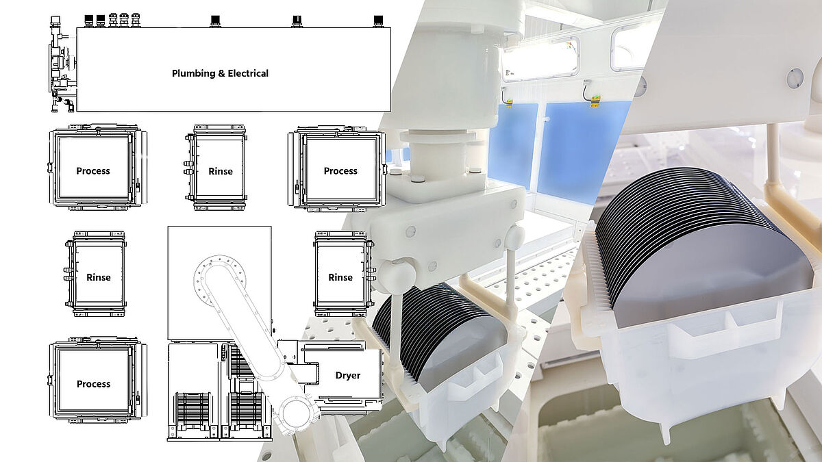
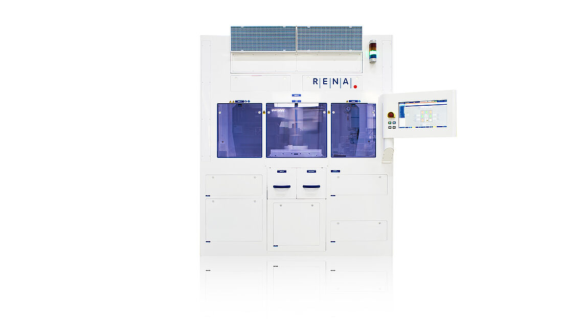
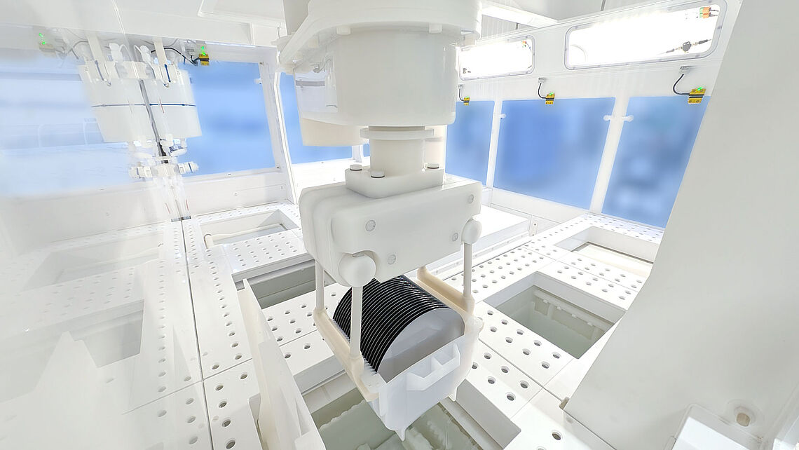
Revolution+ Compact Automatic Wet Processing for Semiconductor Cleaning and Etching

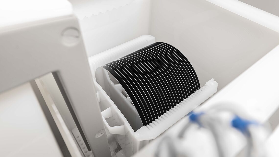
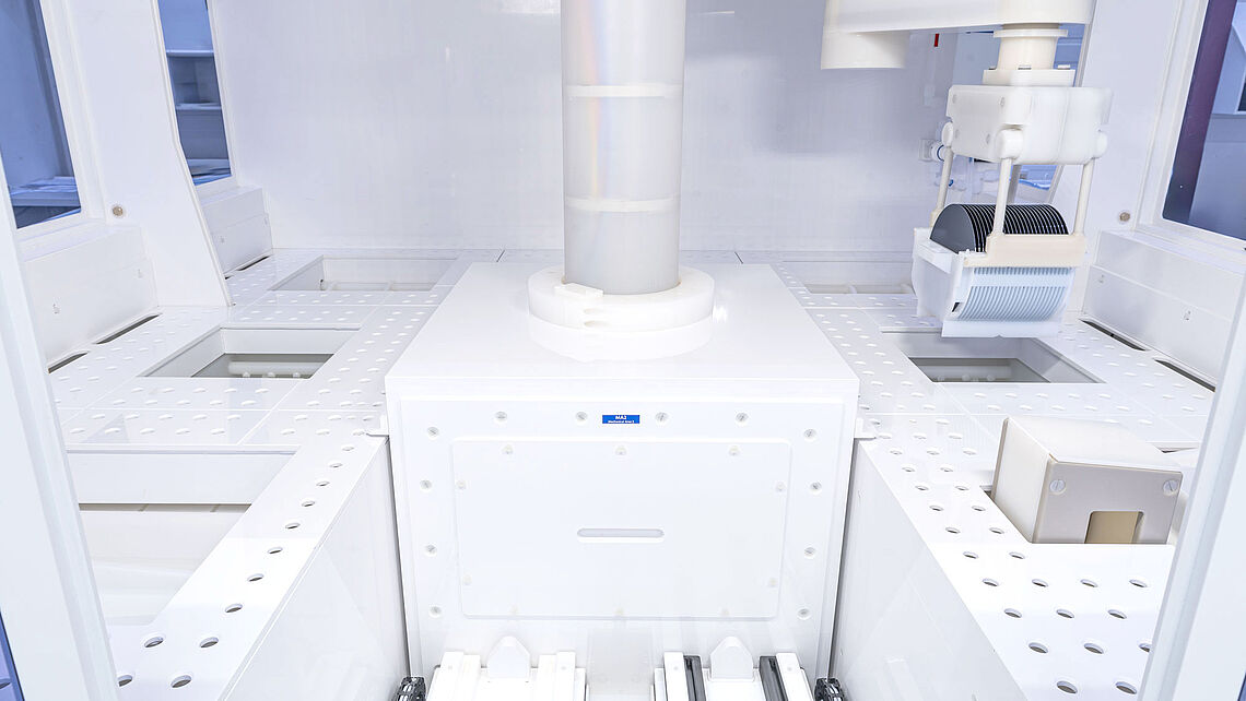
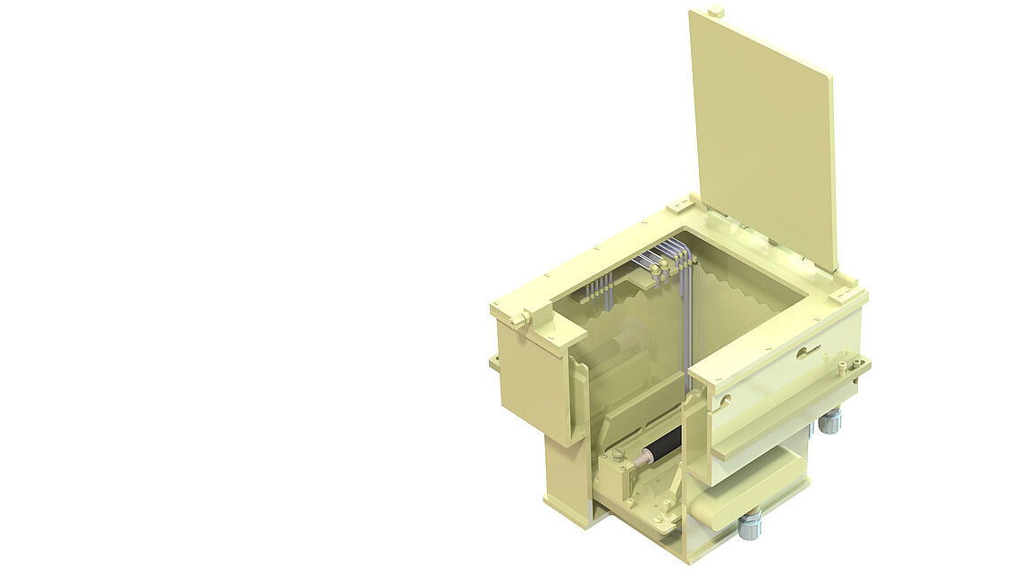
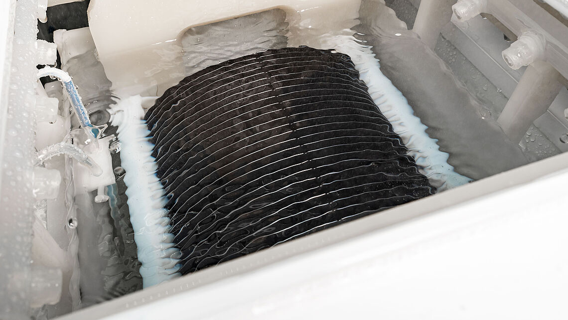
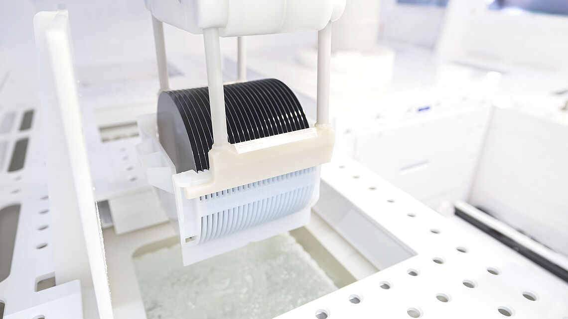
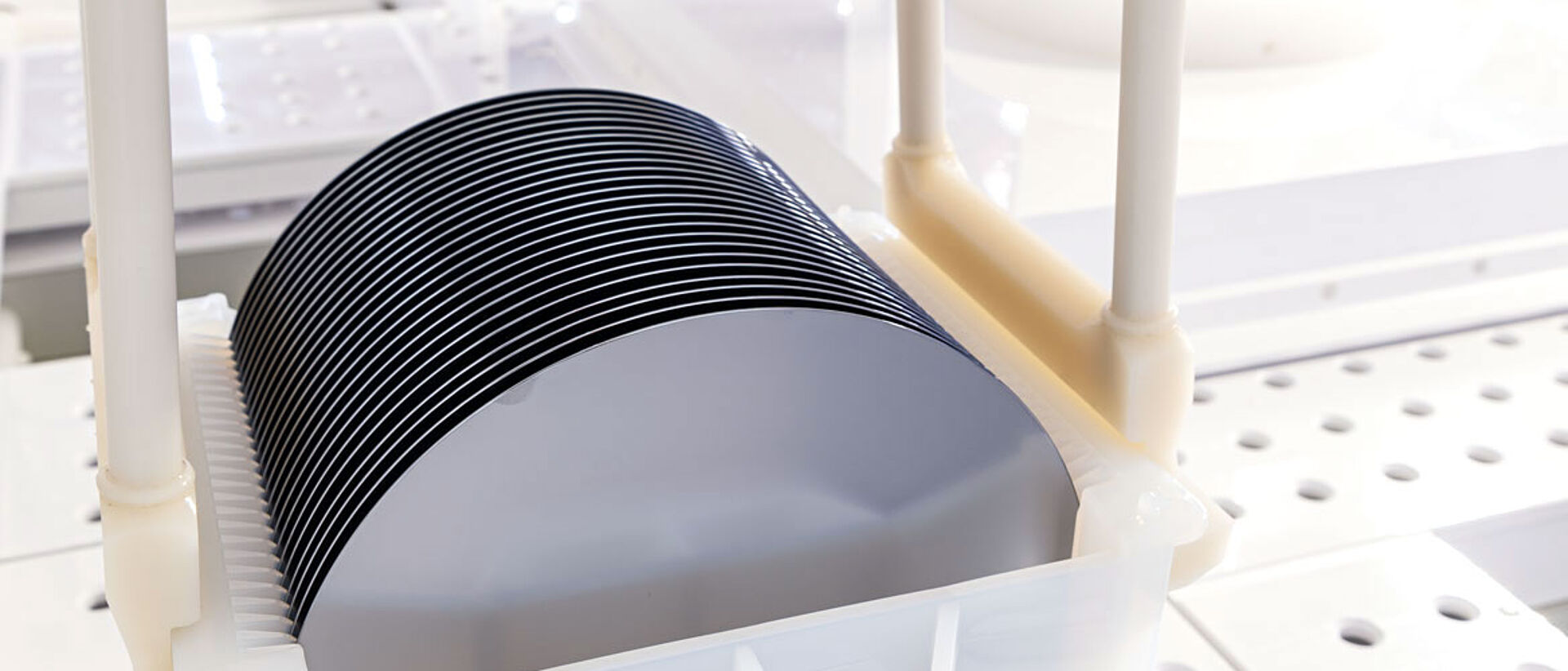
The Revolution+ is a highly versatile automatic semiconductor wet-processing tool designed for semiconductor cleaning, wet etching and semiconductor stripping. Built for flexibility and efficiency, the system combines batch immersion processing with automated wafer handling, enabling reliable chemical processing of advanced semiconductor materials. Depending on individual requirements, Revolution+ accommodates three processing tanks, three rinses, and an advanced Marangoni dryer for optimal results.

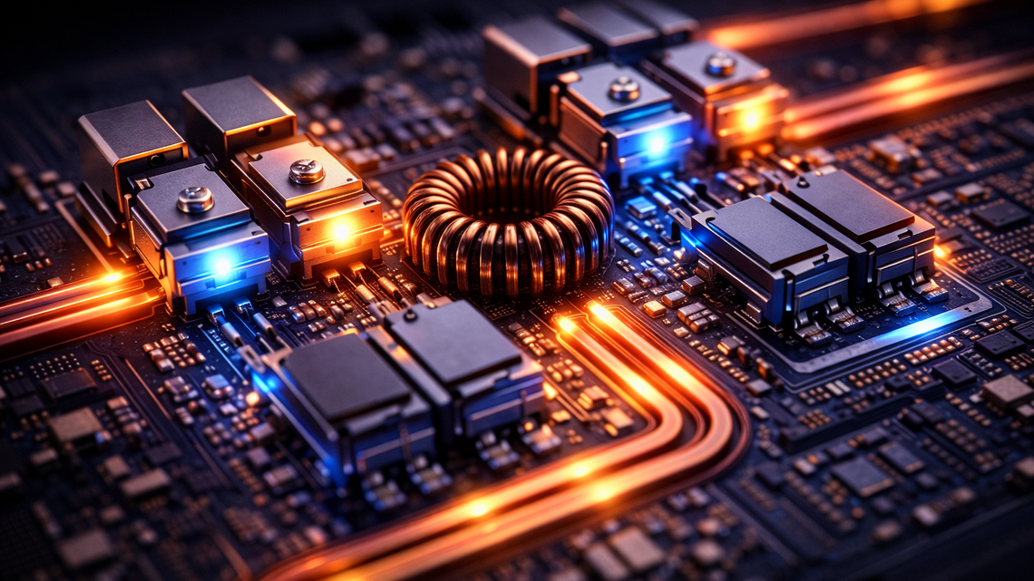
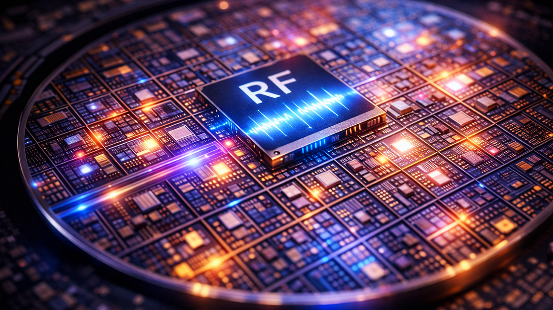
Its compact footprint and modular design make Revolution+ ideal for semiconductor production, R&D environments and pilot lines, particularly for compound semiconductor technologies used in photonics, RF components and power electronics.

RENA REVOLUTION +


CLEVER CONFIGURABLE CUBE
 

  • Compact & versatile
  • Simultaneous processing of 150 & 200 mm wafers
  • 3 Process-Tanks, 3 Rinses, 1 Marangoni dryer
  • Fully automated version available

Automated Wet Processing for Advanced Semiconductor Manufacturing

Semiconductor fabrication requires highly controlled wet chemical processes to remove contaminants, modify surfaces and define device structures.

The Revolution+ wet processing system enables fully automated multi-step processing for wafers, including:

  • Batch immersion wafer processing

  • Semiconductor cleaning

  • Wet chemical etching

  • Photoresist stripping

  • DI rinsing and drying

The system integrates a central rotary robot with multiple process tanks, ensuring efficient wafer transfer between chemical baths while maintaining contamination control.

This architecture enables consistent process results, improved yield and reduced manual handling.

Integrated Marangoni Dryer

RENA’s GenesisX Marangoni dryer offers superior performance, improved yield and reduced particle presence. 


  • Dries hydrophobic and hydrophilic surfaces
  • No damage to photo resist
  • Low IPA usage (< 20 ml per dry cycle)
  • Superior particle performance

Patented TruEtch - Technology

The patented TruEtch process ensures a consistent etch performance, precise etch stability concentration control and increased process reliability. Adding to the versatility of Revolution+ a wide range of applicatons is possible including:

  • Gold etch

  • Aluminum etch

  • Copper etch

  • Buffered oxide etch

  • Surface oxide etch

  • GaAs etch

  • Polysilicon etch

  • Pirahna etch

  • Mesa etch

  • Isotropic etch

  • Anisotropic etch

Flexible Processing for Compound Semiconductor Materials

Next-generation semiconductor devices rely on compound materials with unique electrical and optical properties. The Revolution+ platform supports wet processing for a wide range of substrates and enables compound materials cleaning and wet etching in a single automated platform.

SiC Cleaning

GaN Cleaning and GaN Etching

GaAs Cleaning and GaAs Etching

Silicon carbide wafers require precise 
cleaning steps for power semiconductor 
manufacturing, including MOSFETs and 
high-voltage devices.

Gallium nitride processing requires optimized chemical processes for RF electronics and high-power devices.

GaAs wafers are widely used in microwave electronics and photonic devices, requiring highly controlled wet etching processes.

InP Cleaning and InP Etching

Sapphire Cleaning

Indium phosphide substrates are used in high-speed optical communication components and photonic integrated circuits.

Sapphire substrates are frequently used in LED and optoelectronic manufacturing.

Compact Automatic Semiconductor Processing

The Revolution+ is designed as a small wet-processing tool optimized 
for cleanroom environments where space efficiency is critical.

Key automation features
  • Central rotary wafer handling robot
  • Multi-tank batch immersion processing
  • Automated wafer transfer between chemical baths
  • Dry in / Dry out wafer handling
  • Optional automated loading/unloading

This automated design minimizes particle contamination and ensures repeatable chemical processing.
The system is ideal for:

  • Specialty semiconductor manufacturing
  • R&D semiconductor fabs
  • Pilot production lines


Revolution+ in Front-End of Line Semiconductor Processing (FEOL)

The Front-End of Line (FEOL) is the stage of semiconductor fabrication where transistors and active devices are created directly on the wafer substrate.

Typical FEOL processes include:

  • Wafer cleaning
  • Surface preparation
  • Oxidation
  • Photolithography
  • Wet etching
  • Doping and implantation

Wet processing tools such as Revolution+ are critical during FEOL because surface contamination or particles can directly affect device performance and yield.

The Revolution+ system supports multiple FEOL processes including:

  • Pre-lithography wafer cleaning
  • Oxide removal
  • Surface conditioning for deposition steps

Back-End of Line Semiconductor Processing (BEOL)

After transistor formation, semiconductor manufacturing continues with the Back-End of Line (BEOL) stage. 
BEOL focuses on creating the metal interconnect layers that connect devices into complete integrated circuits.

Typical BEOL wet processes include:

  • Residue cleaning after etching
  • Surface preparation before metallization
  • Post-etch cleaning
  • Chemical stripping of photoresist layers

The Revolution+ enables reliable cleaning and wet etching processes for BEOL applications, ensuring high reliability of interconnect structures.

Applications

The Revolution+ wet processing system supports semiconductor manufacturing across multiple advanced technology sectors.

Photonics

Processing of InP and GaAs wafers for optical communication devices, lasers and photonic integrated circuits.

Power Electronics

Cleaning and wet processing of SiC and GaN wafers for power semiconductors used in electric vehicles, renewable energy and industrial power systems.

RF Components

GaAs and GaN devices used in RF amplifiers, radar systems and wireless communication technologies.


Advantages of the Revolution+ Wet Processing System

The Revolution+ platform combines automation, process flexibility and compact design for advanced semiconductor wet processing.

Key benefits

  • Fully automatic semiconductor cleaning and wet etching
  • Outstanding Drying-Capabilities
  • Multi-step chemical processing in one tool
  • Flexible support for 150 and 200 mm compound wafers
  • Modular versatile platform
  • Compact footprint for cleanrooms
  • High process repeatability

This makes the Revolution+ a reliable solution for advanced semiconductor fabrication environments.

Frequently Asked Questions

The system supports processing of several advanced materials including:

  • Silicon Carbide (SiC)
  • Gallium Nitride (GaN)
  • Gallium Arsenide (GaAs)
  • Indium Phosphide (InP)
  • Germanium (Ge)
  • Sapphire substrates

Compound semiconductor technologies are widely used in:

  • Power electronics
  • RF communication
  • Photonics and optical communication

Semiconductor wet processing refers to the use of chemical solutions to clean, etch or strip materials from semiconductor wafers during manufacturing.

Wet etching is a process where chemical solutions selectively remove material from the wafer surface to create device structures.

SVP Sales
Jay Johnson