What is wet etching of wafers?
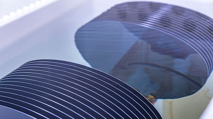
In wet etching, a layer on the wafer is selectively removed using a chemical liquid. The chemical reacts with the material and dissolves it, allowing it to be etched away.
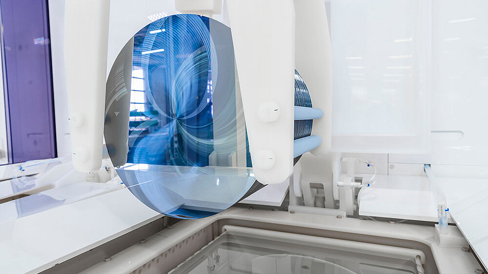
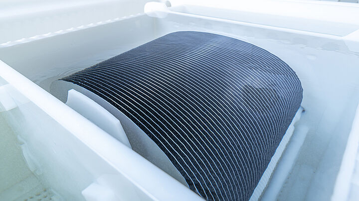
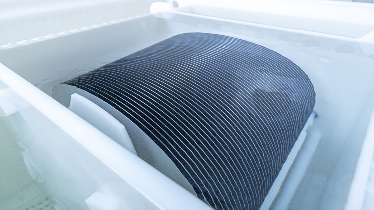
During the process, the wafer is either immersed in an etching solution or wetted with it. The solution only attacks the unprotected areas and removes material there. The areas that need to remain are protected beforehand by a masking layer – for example photoresist or oxide.
A major advantage of wet etching is that it can be highly selective: the chemicals used can be chosen to specifically attack certain materials, while leaving other layers as unchanged as possible.
What needs to be considered when etching wafers?
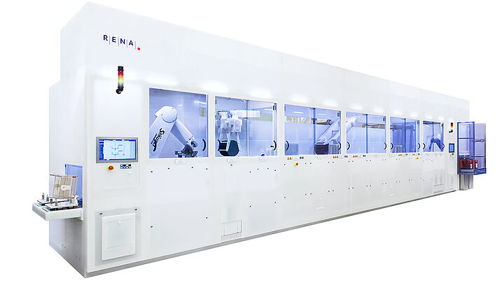
RENA Technologies has many years of experience in wet-chemical wafer processing and the process expertise required to achieve optimal etching results for a wide range of materials and substrates. For each application, specific etchant mixtures are used and carefully matched to ensure compatibility with the respective layers. High selectivity is essential in order to reliably prevent unwanted material removal from adjacent or underlying layers.
Wet-chemical etching processes place high demands on the protective mask or resist layer. RENA Technologies considers not only the selection of a suitable resist, but also the etching medium used, the etching time, and the etching temperature, which significantly influences the reaction rate. In addition, the adhesion properties of the resist on the respective substrate are taken into account during process design to prevent undercutting or structural loss.
During the process, wafers are immersed in 7an etching solution or wetted with it. The chemical reacts selectively with the unprotected areas of the material, while masked areas remain reliably protected. Since wet-chemical etching often shows isotropic etching behavior, potential lateral material removal is already taken into account during process development.
To ensure maximum process stability and quality at all times, the etching chemistry and process parameters are thoroughly examined in extensive tests in the RENA R&D laboratory. The optimal composition of the etching solution as well as the complete process flow are individually tailored to each application.
After wet-chemical etching, intensive multi-stage rinsing with deionized water (DI water) is performed. This completely removes etchant residues – including those that have penetrated the resist layer – and reliably prevents subsequent resist damage or delamination.
Key factors in wafer etching:
Many years of process and equipment expertise from RENA Technologies
Application-specific etchant mixtures for different materials
High requirements for mask and resist layers
Control of: etching medium, etching time, etching temperature
Consideration of isotropic etching behavior and undercutting
Process development and optimization in the RENA R&D laboratory
Thorough DI-water rinsing after the etching process
Why is wet etching the economical and process-stable solution for semiconductor manufacturing?
Wet-chemical etching processes offer key economic advantages in semiconductor manufacturing – especially when based on the many years of process and equipment expertise of RENA Technologies. Compared to plasma-assisted dry etching processes, wet etching enables high etch rates, short process times, and therefore efficient utilization of production capacity.
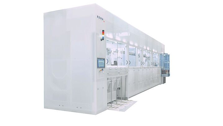
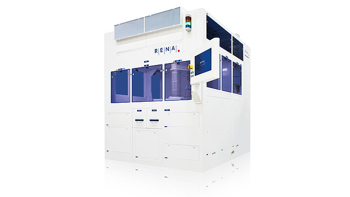
The wet-chemical systems developed by RENA Technologies feature robust yet flexible equipment technology. They are consistently designed for high throughput, process stability, and reproducibility in volume production – while maintaining low operating costs.
Especially for high-volume manufacturing processes, wet etching is therefore a highly cost-effective solution. Combined with comprehensive process know-how and individually tailored applications, RENA Technologies enables selective and reliable layer removal, reproducible surface preparation, and stable, efficient series production.
Even in the era of highly advanced dry etching technologies, wet etching remains an indispensable part of modern semiconductor processes. With the wet etching solutions from RENA Technologies, customers benefit from maximum process reliability, high product quality, and sustainable cost-efficiency in the production of high-performance and reliable semiconductor devices.
- High etch rates and short process times
- High throughput in volume production
- Stable, reproducible processes
- Low operating costs
- Indispensable for modern semiconductor manufacturing