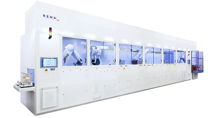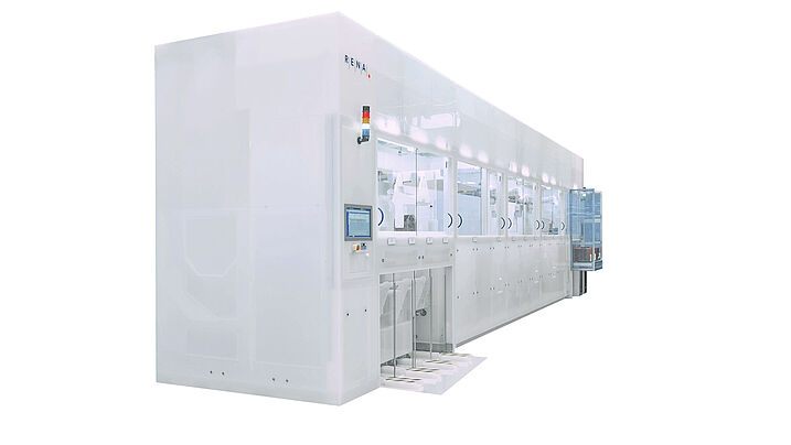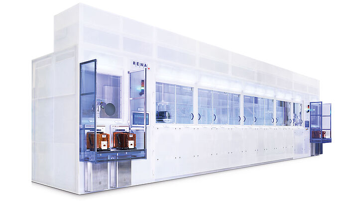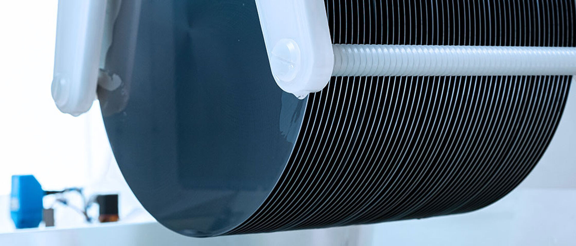
High throughput surface treatment of bare semiconductor wafers for wafer fabrication
The first and a crucial step in semiconductor manufacturing is wafer fabrication. The surface quality and cleanness of bare i.e. un-patterned wafers are of fundamental importance for semiconductor device quality. RENA manufactures fully automated wet benches for surface cleaning and etching of semiconductor wafers, delivering high throughput, high yield, precise process control as well as outstanding surface treatment results. Our equipment are capable of processing 200 mm as well as 300 mm wafers, with or without carrier using full- or half-pitch wafer cassette. The chemical stations can be adjusted to customer process requirements and the wafer material including mono crystalline silicon (Si), germanium (Ge), gallium arsenide (GaAs) and gallium nitride (GaN).
RENA’s bare wafer processing platforms can be employed after lapping, after chemical mechanical polishing (CMP), prior to epitaxial growth and at the final cleaning step. Our equipment are also suitable choice for wafer reclaim to recycle the already patterned semiconductor wafers.