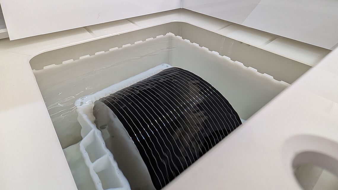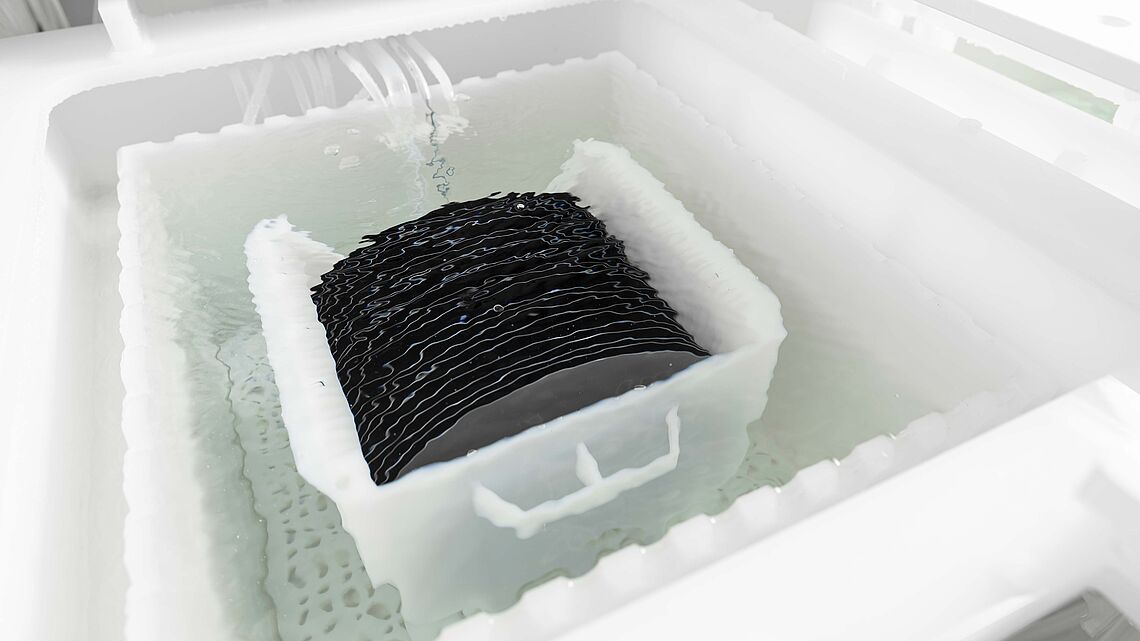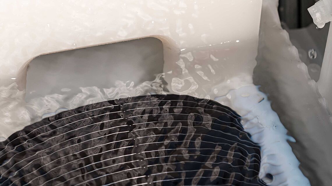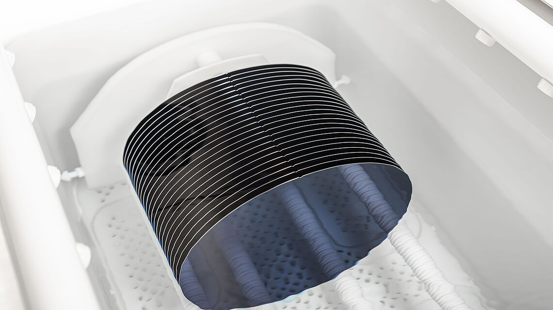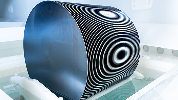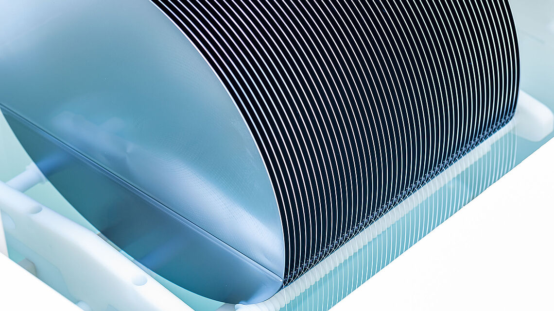
Photonics Wet Processing Solutions

Precision Wet Processing for Advanced Photonics

Photonics is rapidly gaining traction in semiconductor manufacturing as traditional scaling approaches reaching their physical and economic limits. To overcome the constraints of Moore’s Law and achieve much faster, more energy-efficient data transmission—both between and within chips—optical technologies are becoming indispensable. This transition accelerates the adoption of compound semiconductors and complex multi-material stacks, bringing new challenges in surface control, material selectivity, and yield optimization.

RENA provides wet processing solutions specifically designed to address these requirements. By combining process expertise with advanced equipment technology, we enable reliable, high-uniformity processing for sensitive photonic structures.

Challenges in Photonics Processing

In photonics, even minor deviations in surface or material properties can directly impact device performance. Typical challenges include:

  • Surface roughness after wet etching, particularly during HF-based oxide removal 
  • Non-uniform oxide stripping leading to refractive index variations 
  • Particle redeposition during wet cleaning steps 
  • Limited uniformity across wafer batches 
  • Insufficient selectivity in multi-material systems 
  • Anisotropic etching behavior where precise structuring is required 

Increasing process complexity and material diversity continue to push conventional approaches to their limits.

RENA Approach: Controlled Wet Processing

RENA addresses these challenges by rethinking wet processing as a controlled and highly engineered process step. Our approach is based on:

  • Improved handling for fragile compound semiconductor substrates
  • Precise control of chemical interactions at the wafer surface 
  • Optimized fluid dynamics to ensure uniform treatment across all wafers 
  • Process integration tailored to photonics device requirements 


This enables consistent results in terms of surface quality, selectivity, and reproducibility—key factors for scalable photonics production.

Core Capabilities

Surface Conditioning and Cleaning

RENA offers optimized cleaning solutions for compound semiconductors such as InP and GaAs.

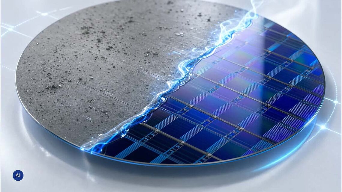
Post-CMP and post-EPI cleaning processes are designed to remove residues while preserving surface integrity. Surface roughness and stoichiometry remain unchanged, ensuring stable optical properties.

Etching and Structuring

Our batch processing platforms enable high-uniformity wet etching for:

  • III-V mesa structures 

  • Undercuts and 3D geometries 

  • Metal layers and complex stack systems 

In addition, RENA develops selective etching approaches that allow controlled processing across different materials within a single structure.

Lift-Off and Resist Removal

Batch metal lift-off processes are optimized for fragile wafers and sensitive layers. The focus lies on minimizing mechanical and chemical stress while ensuring complete removal.

Surface Passivation and Repair

Wet chemical passivation processes can be used to reduce vacancy defects and repair damage caused by dry etching. This contributes to improved device performance and long-term stability.

Advanced Material Processing

RENA supports specialized processes such as porous material formation, enabling new functionalities in photonic devices.


Materials Expertise

Our processes are developed and validated for key photonics materials, including:

  • Indium Phosphide (InP) 

  • Gallium Arsenide (GaAs) 

  • Germanium (Ge) 

  • Silicon Nitride (SiN) 

  • Silicon (Si) 

Process Portfolio

Unique Photonics Solutions

RENA solutions are specifically designed to overcome common limitations in photonics wet processing:

  • Surface roughness control: Optimized chemistries ensure smooth surfaces even after oxide removal 

  • Uniformity: Advanced batch processing guarantees consistent results across wafers 

  • Particle control: Minimized redeposition through optimized flow and rinsing strategies 

  • Selectivity: Tailored processes for multi-material stacks

  • Process stability: Reproducible results for high-yield manufacturing

RENA Wet Processing Steps for Photonics

The covered range of wet processing steps required in photonics manufacturing:

  • RCA and Piranha cleaning 

  • Buffered oxide etching (BOE) and anisotropic etching 

  • Surface smoothening 

  • Photoresist stripping 

  • Marangoni drying for residue-free wafer surfaces 

Applications

RENA wet processing solutions support a wide range of photonics applications:

  • Optical transceivers 

  • Silicon photonics integration 

  • Laser diodes (InP, GaAs) 

  • Waveguides and modulators 

  • Sensor and LiDAR technologies 

Why RENA

RENA combines equipment engineering with deep process expertise in wet chemistry. Our solutions are designed for industrial production, with a strong focus on uniformity, surface quality, and reliability.


Get in Touch

If you are working on photonics devices and facing challenges in wet processing, we are ready to support you.

Contact our experts to discuss your application or request a process evaluation.

  • Contact us → /contact 

  • Explore wet processing solutions → /wet-processing 

  • Semiconductor applications → /semiconductor 

  • Cleaning technologies → /cleaning-technologies 


Frequently Asked Questions

It is the use of liquid chemicals to clean, etch, strip, develop, or otherwise prepare wafers and device surfaces during photonics fabrication.

Photonic devices are very sensitive to surface contamination, residue, and damage, so wet steps help control yield, optical loss, and device uniformity.

Common steps include wafer cleaning, wet etching, photoresist stripping, oxide removal, metal lift-off, and surface activation or preparation before later steps.

Yes, it is central in advanced packaging, photonics, MEMS, RF, and compound semiconductor production because many key removal and preparation steps still depend on liquid chemistry.

SVP Sales
Jay Johnson